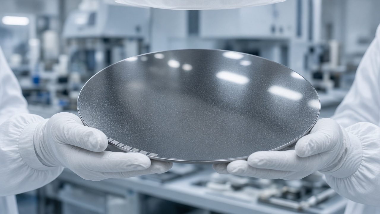
The Japanese chemicals and materials group announced the result on 15 September 2026. It calls 300 mm among the world's largest SiC substrate sizes under development and, on its August 2026 research of public information, a first in Japan. Today's commercial mainstream remains 150 mm epitaxial wafers, with 200 mm shipments already under way.
TL;DR: Resonac grew 300 mm SiC crystals, a step toward larger, cheaper power-device wafers. Factories still run mostly on 150 mm, with 200 mm starting. Uses target EVs, renewables, data-centre power and AI heat spreaders. Do not confuse a lab-to-process milestone with shelves full of 12-inch SiC chips.
Status note: Checked 29 September 2026 against Resonac's 15 September news release. Yield, pricing and customer qualification timelines are not in the release. Treat competitor size claims as company-researched, not independently audited here.
Why wafer diameter matters
Silicon carbide cuts power-conversion losses and heat versus ordinary silicon in many high-voltage jobs. Bigger wafers can mean more devices per slice and lower unit cost if quality holds. Moving from 150 mm to 200 mm is already the industry's near-term race. 300 mm is the next engineering hill: harder crystal growth, harder processing, higher payoff if it works at scale.
Resonac frames the work inside Japan's NEDO Green Innovation Fund project on next-generation SiC wafers for green power semiconductors. Public funding and private process know-how are both in the story.
Where the material goes
Demand cited by the company sits in electric vehicles and renewable power conversion, and in efficient power supplies for data centres. High thermal conductivity also makes SiC interesting as a heat-spreading or advanced packaging substrate for AI servers and high-performance computing. A high refractive index keeps AR smart glasses on the longer-range candidate list.
None of that requires every car inverter to use a 300 mm-derived die in 2026. It does explain why materials firms race diameter: the same chemistry serves several growth markets.
What would change the read
Qualified 300 mm epi supply contracts, published defect densities, or a major device maker's process of record would move this from milestone to manufacturing story. Until then, investors and engineers should file it under substrate roadmap, not product launch.
Sources: Resonac, Successfully Develops 300 mm SiC Single-Crystal Substrates.