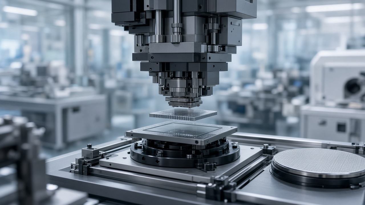
TL;DR: Applied Materials is teaming with Besi at the EPIC Center in Silicon Valley to widen R&D on AI chip packaging, including 3D logic-plus-memory stacks, panel-level integration, thermo-compression bonding, and co-packaged optics. Applied could invest up to roughly $5 billion in stages and aims to prepare operations within a year. This expands a research partnership, not a consumer chip shipping next week.
Status note: Checked 2 October 2026 against Chosun Biz reporting dated 2 October 2026 on the Applied and Besi EPIC Center agreement. Investment figures and timelines are company-stated targets; fab tool orders and customer adoption can slip. No new retail GPU or phone chip is announced as a direct product of this release.
Why packaging suddenly sits next to lithography headlines
Moore's Law slowing at the transistor level pushed performance gains into how dies are stacked, connected, and cooled. AI accelerators need memory close, bandwidth wide, and power delivery stable. That turns chip packaging from a back-office step into a front-page bottleneck, especially for high-bandwidth memory stacks and multi-die logic tiles.
Besi, a Dutch equipment specialist strong in hybrid bonding, opened the EPIC Center in Silicon Valley as a collaboration hub where chipmakers and tool vendors prototype integration flows before they commit full fabs. Applied Materials, the largest U.S. semiconductor equipment firm by reach, already sells deposition, etch, and inspection tools across every major fab. Joining EPIC as an innovation partner links Besi's bonding expertise with Applied's breadth in front-end and advanced packaging lines.
What the partnership adds beyond hybrid bonding
Chosun Biz reported that the expanded work goes past hybrid bonding into next-generation interconnects, three-dimensional integrated circuits that combine logic and memory, panel-level integration, thermo-compression bonding, die-to-wafer and die-to-die assembly, and co-packaged optics. That list reads like a roadmap slide for AI systems in 2027 and 2028, when photonics and chiplets move from niche papers to factory flows.
Panel-level integration, for example, tries to process many packages on a large panel instead of one wafer at a time, aiming for cost and throughput wins if yields hold. Thermo-compression bonding uses heat and force to join dies with fine pitches, a workhorse for high-density stacks. Co-packaged optics brings fiber links closer to silicon to cut electrical losses on AI clusters that otherwise drown in copper reach limits.
Applied's staged investment and timing
Applied may invest up to about $5 billion in the EPIC center in stages, according to the same reporting. Staged checks are common when a toolmaker funds shared cleanroom space, prototype lines, and early process kits before knowing which customer nodes will pay back first. The aim is to prepare operations within a year, a fast calendar for semiconductor R&D hubs that often spend longer on permitting and tool install.
Five billion dollars is a headline number, not a single wire transfer tomorrow. Applied historically spreads capex across quarters and ties milestones to customer co-development. Readers should watch SEC filings and earnings calls for how much actually lands in fiscal 2027 versus option value for later tranches.
What CEO Gary Dickerson emphasized
Applied chief executive Gary Dickerson framed the deal as expanding interconnect collaboration to support AI systems, language that mirrors how cloud vendors press suppliers for end-to-end bandwidth, not just faster transistors. Interconnect here means the vertical and horizontal wires, bumps, and optical paths that let many dies behave like one super-chip.
For Besi, Applied's brand pulls more U.S. chip designers and foundries through the EPIC doors. For Applied, Besi's bonding leadership fills a gap in the portfolio where organic internal projects might move slower alone. Neither company claimed a finished product win on Tuesday; they claimed a wider lab bench.
How this fits the AI supply chain
Nvidia, AMD, Intel, and custom cloud silicon teams all depend on packaging houses and tool vendors to translate architecture slides into shippable modules. When HBM stacks sit on logic, yield loss at the packaging step can waste perfectly good wafers. That is why equipment partnerships now get CEO quotes on the same day as earnings from memory makers like Micron.
This announcement is R&D partnership expansion, not a binding order for every AI chip in 2026. Customer fabs still choose whether to adopt panel flows or co-packaged optics for each product generation. Export controls and China-U.S. tool restrictions can also reshape where joint labs locate and who may walk the floor.
Partnerships at this scale also tell policymakers that advanced packaging is strategic infrastructure, much like lithography and memory fabs. That political layer was not in Tuesday's release, but it often follows when multi-billion-dollar lab bets land in Silicon Valley.
Where things stand
On 2 October 2026, Chosun Biz reported that Applied Materials joins Besi as an innovation partner at the EPIC Center in Silicon Valley, broadening research beyond hybrid bonding to next-gen interconnects, 3D logic and memory, panel-level integration, thermo-compression bonding, die-to-wafer and die-to-die work, and co-packaged optics. Applied may invest in stages up to about $5 billion and targets preparing operations within a year, with CEO Gary Dickerson citing expanded interconnect collaboration for AI systems.
What is not promised is a named AI accelerator hitting retail on a fixed date, guaranteed returns on the full investment envelope, or industry-wide adoption timelines. The move widens shared packaging research; mass production wins still depend on customer nodes and yield proof later.
Sources: Chosun Biz on Applied Materials and Besi EPIC Center partnership, 2 October 2026.